Every undergraduate in the School of ECE at Georgia tech is required to take a two-semester senior design course. The first semester is mainly spent learning about topics in ethics, business, statistics and probability that are of use to those practicing engineering. Additionally, students select or create a project to complete during the second semester of the course. While there were some very interesting projects proposed by various professors and members of industry, I really wanted to work on my own project, not somebody else's. Me and a couple classmates met and I proposed working on a fuel economy estimator for vintage cars (that I could use on my vintage VW beetle). We proposed the project, found a professor that agreed to advise us, and submitted it for approval by the professors who run the ECE senior design course.
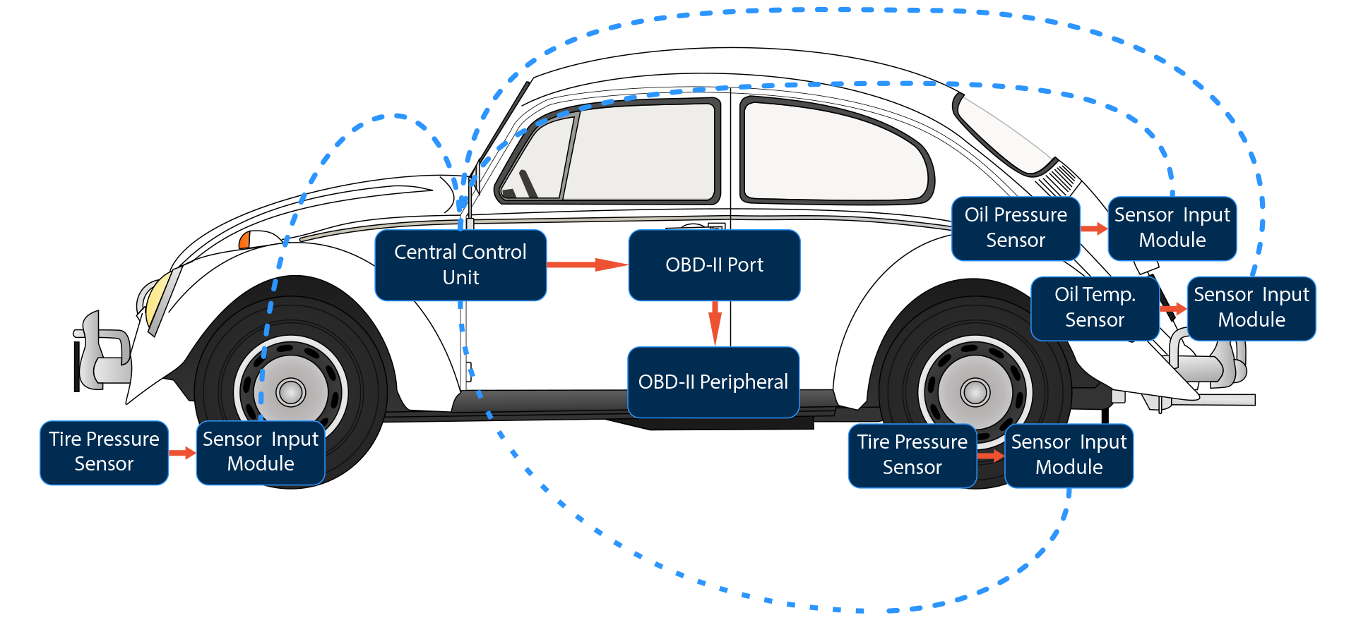
The idea went through a major change sometime near the end of the second semester which made it much more generic of a solution. We decided that we would make a generic sensor interface which wirelessly transmits car sensor data to a central "ECU" of sorts that would expose the data an OBD-II interface. This would mean that the sensors that were added to the car could be used with any off the shelf OBD-II peripheral, from insurance monitoring systems, to wireless Bluetooth gauge clusters and dataloggers. However, this meant that our solution would need to be able to interface with a multitude of sensors.
What resulted was the most complicated piece of electronics I've ever designed or built, and an extremely challenging (yet engaging) four months for me and my team. -- This entry is split into two parts. This covers the problem and the circuits I designed. The next part covers the board layout, construction of the boards, programing, and the end results. If you'd like to jump to that part, click here.
the problem(s)
While aftermarket gauges are very common addition to a large number of project cars, the data is "locked" into the gauge itself. This means that the only thing I can do with the data is read it with my eyeballs. Oftentimes the data collected from one sensor is not enough to tell a complete story. For example, low oil pressure can be an indicator of excessive main bearing wear, but the single datapoint of oil pressure = 20 psi reveals very little information as oil pressure can be highly dependent on oil pressure: as the engine turns faster, so does the oil pump, which increases oil pressure. For my VW, oil pressure should be roughly 10 psi per 1000 RPM. I have no way with my current gauge cluster to see this on a gauge or record the information, other than looking at the two gauges and doing the math in my head. Essentially, the main problem is there is no way to expose this data to any other interface to which it might be useful to record or use in different ways.
Another problem we wanted identified was the pain of wiring new sensors into a vehicle. While not a huge amount of effort, the routing of wires and installation of gauges may require permanent modification to the vehicle (drilling holes in the body or the dashboard) which may make some car owners (especially classic car owners) nervous to add sensors to their vehicle. We wanted to see if we could remove this necessary step in sensor installation.
the solution
We eventually settled on creating a wireless sensor interface that exposes the data over the automotive industry standard debug interface; the OBD-II port. Sensors would connect to modules that would be responsible for reading the sensor data. These would be easy to wire as twelve-volt power should be readily available almost everywhere in the vehicle that sensors need to be placed (mainly inside engine compartment), and would be located close to the sensor for minimal visible wiring. The sensors would then relay their information periodically to a central board which then communicates with any OBD-II peripheral that may be connected. To simplify the project and preserve its genericness, the "central control unit" would have no displays, gauges, or outputs, other than the OBD-II port. If the user wanted to see their oil pressure, then some OBD-II monitoring solution would need to be used with our board.
What's interesting, is that with our idea/solution, even though we had pivoted from the MPG estimation project, we could still estimate MPG by combining fuel consumption (using a flow sensor) and speed (using a rotary encoder on the speedometer cable, or a GPS module).
sensor interfacing
A difficult problem was identifying the common modes that automotive sensors communicate over. After extensive research, we settled on supporting voltage, resistive and digital (PWM and PFM) sensors. There are plenty more interfaces that were a bit more esoteric (bi-state current?), but we figured the three we chose were enough to cover a wide variety of sensors. We identified early on that we wanted to interface with my existing Speedhut oil pressure and oil temperature sensors (one outputs a voltage and one outputs a resistance), as well as a digital flow sensor we found.
Another problem was powering the sensors. While the resistive sensors wouldn't need to be "powered," the the voltage and digital output sensors would likely need to be. While I wish I had had enough time to prototype and build a continuously variable linear supply, I instead opted to just support four different common voltages, 1.8V, 3.3V, 5V and 12V.
design :: ccu
Though some particular elements of the design evolved during the circuit design process, I had the basic idea sometime in late January or early February. With that, I went into a frenzy with my group-mate Evan, I taught him the basics of Eagle so we could build the library together for the project, and we were off.
overview
The CCU is the simplest of the two boards I designed. There is some power supply protection circuity, and a pretty simple regulator setup. For this board we went with the mbed microcontroller board, since the majority of the software could be written before the boards were done by another member of my team. Connected to the mbed are two wireless transceivers, one for the 433MHz band and one for the 915MHz band, a CAN bus transceiver with some protection circuitry, and an SD card. There's also an RGB led (because why not), and two seven segment displays for a basic user interface to do board setup.
power supply input protection
A vehicle is a pretty nasty environment for electronics. Newer cars have relatively complex power conditioning circuitry, but in older cars there's likely nothing more than an alternator, a rectifier and the battery. I read a few papers which suggested load-dump conditions (lights turning on and off, etc) causing voltage spikes up to a hundred volts. Additionally, we wanted our boards to not fry when potentially plugged in backwards. I used this circuit I found in an app note from Texas Instruments entitled Step-Down Converter with Input Overvoltage Protection, and added an extra MOSFET (Q1A) at the input to protect against reverse power input polarity.
When the power is connected with the correct polarity, the body diode forward biases and the gate becomes biased below the source, which reinforces the FET on. When the supply is connected with reverse polarity, the body diode does not conduct, and the reverse polarity actually biases the FET further into a nonconducting mode. Zener Z1 (as well as Z3) protect the gate-source junction of the FET.
Q1B in conjunction with the two BJTs disconnect the entire board from th input when Z2 reverse biases. When Z2 goes into reverse breakdown and Q3 and Q2 conduct, connecting the gate of Q1B to its source, which turns Q1B off. If I had to do this again, I would instead build a input clamping circuit instead of an input "cutoff" circuit. To prevent the entire board going to sleep in an overvoltage condition, I slapped a big bulk capacitance after the cutoff circuit to hopefully keep the board alive during any transients.
The overvoltage condition output allows the microcontroller to sense when there has been an overvoltage condition so that it can potentially sleep any high-power devices to extend the time that the bulk capacitance can sustain the board. The jumper was there in case the protection circuitry didn't work at all (I hadn't worked out the bias resistor values before I sent the boards out), so I wanted an easy way to bypass the circuit entirely.

regulation
I used an LT3493 buck regulator from Linear followed by a linear regulator to provide lower power supply ripple. Most likely unnecessary, but it couldn't hurt. The buck regulator regulates the 12V input to 4.5V, which is then input to the linear regulator (an LD291 from STMicro). This keeps the power loss in the linear regulator to a minimum (as opposed to linear regulating the 12V input).
The only interesting thing about the use of the buck regulator is the diode-or gate which drives the shutdown pin of the buck regulator. The mbed drives the BUCK_ENABLE signal, while the keyed 12V line in the car (only present when the key is in the ignition/on position) drives the SWITCHED_SUPPLY_IN signal. The only way the board can be woken from sleep is when the driver turns the key on in the car. The first thing the mbed does on power-up is assert its buck enable line. The mbed monitors the switched supply line to determine when the key has been turned off, finishes any writes to the SD card, communicates to the sensor boards that the car is turned off, and then goes to sleep by de-asserting its buck enable signal.
Everything else is out of the datasheet for the regulator. I did add a zero ohm jumper resistor to the shutdown line so I could permanently enable the regulator in case the sleep feature didn't work. Actually, there's a lot of zero ohm resistors throughout the schematic. I used them whenever I was unsure at all if a feature was going to work. This let me be more sure that this first revision of the boards would be somewhat workable before the semester was over. There wasn't enough time in the semester to design, build, program, and test the boards, and then do a second revision. They had to work the first time.

CAN bus termination
At a minimum, the CAN bus must be 120 ohm terminated.
I did a little more than necessary, since the only other device on the bus will be the OBD-II peripheral, over a few milimeters of wire (as opposed to 50 devices over an entire car). The CAN transceiver I used (the SN65HVD23x from TI) has a VREF output, which is regulated to half the power supply voltage. This can be used to stabilize the common-mode voltage on the CAN bus. To do this, the termination is split and the reference voltage is connected in the middle. I also used a transient voltage suppression diode package that was intended for use in CAN bus transient suppression. Lastly, there are two capacitors which form an optional filter network in case the slew rates were to high on the bus lines.
There's also an empty symbol which holds the mounting holes that need to be cut out to mount the male OBD-II connector. I didn't want to solder wires directly into the board from the male connector (like is done here), so I added an additional connector to place behind the OBD-II connector (connector-ception), so that the OBD-II connector can be readily mounted and unmounted from the board.

wireless transceivers
There are two transceivers that we placed on the board. One operates in the 433Mhz band, and was really only put there as a "stretch" goal to get our board communicating with off the shelf tire pressure monitoring systems. The 915Mhz transceiver we used for communication between the boards. We used the MRF89XAM9A from Microchip. There's a myriad of these things available, and they all probably would have worked for what we needed them for, but I really like thorough documentation, and this module from Microchip had some of the best.
full ccu schematic
That's about all of the most interesting parts of the CCU board. The rest is pretty basic microcontroller interfacing stuff. I had to use an I/O expander to interface the seven segment displays and RGB LED. I actually found one that had PWM outputs so I could control the color of the LED. If you're interested in the whole thing, there's a PDF you can view here.
design :: wsb
The more complicated and interesting design was the board that interfaces to the sensors. There were some additional constraints here that made it much more interesting to figure out. As stated before the board needed to interface with voltage output, digital output and resistive output sensors, so a fairly complex analog front-end was needed to ensure accurate readings. I also didn't want to rely on the keyed ignition line being available throughout the car, so the power supply needed to have a very low-current sleep mode as well that could be enabled by the microcontroller.
power supplies
The same protection, buck and linear regulator are present from the CCU, but I placed down an additional low-current linear regulator (10mA maximum) which linear regulates from 12V down to 3V. To get the board to consume very little power during sleep, I used an auto-switching power multiplexer from TI. This muxes two power supplies, always switching in the one that is at a higher voltage. Every IC on the board other than the microcontroller is powered from the main 3.3V linear regulator, so when the microcontroller puts the buck to sleep, the 3.3V supply falls to 0V, the and mux switches in the 3V supply to keep the microcontroller alive when as it goes into a sleep state.
Every so often the microcontroller wakes up, listens for incoming packets from the CCU board, and if nothing is heard within a few milliseconds the board goes back to sleep for a few seconds. This reduces the average sleep current to microamps, instead of 50+ milliamps. This took a bit of work to get functioning, but I'll cover that later.

I didn't have enough time to design and build an adjustable power supply to power the sensors, so instead I took the brute-force approach and placed four linear regulators on the board, each at different output voltages: 12V, 5V, 3.3V and 1.8V. As the battery voltage in the car may at times be below 12V, to be able to rely on the 12V source, I needed to boost a bit above the input voltage to ensure there was always enough headroom to linear regulate to 12V. I placed a boost converter from Micrel (MIC2288) on the board to boost to 14V, which powers the 12V and 5V linear regulators. I used the common LM217 for the linear regulators.

sensor supply mux
We wanted to allow the microcontroller to pick which supply it powers the sensor with, so that the user can setup the board via software or DIP switches for different sensors that may require different supply voltages. I found this part from Vishay, the Si3865DDV, which is essentially a p-channel MOSFET switch with a n-channel MOSFET to drive its gate. This allows for a low-voltage control of a higher voltage. Since the output of each switch is chained together and connected to the sensor, two of these parts need to be used back to back to switch each supply. This prevents the body diode of the high-side p-channel MOSFET from reverse biasing, and shorting the regulators together. I added a final "gate" switch which can disconnect the sensor power supply with one signal.
There are some optional resistors which form a low-pass filter network with the 1000pF caps to control the slew rate on the output of the switch.

analog front-end
This is where I spent most of the time. I wanted to have a way to measure a large range of resistances and a large range of voltages, as well as support digital inputs. After stumbling upon a few vintage app-notes that covered building simple multimeters, I took what I could and cobbled something together that could be controlled from the microcontroller.
While I could have picked the highest input voltage that would be expected from a sensor (12V from a 12V sensor), and then used a fixed voltage division ratio to divide the voltage down within the range of the A/D converter, this would mean that 1.8V sensors would only be utilizing a very small portion of the A/D converter's conversion range, which felt like a sloppy solution. I created a variable division ratio voltage divider by using a hex-buffer (a 74xx series part) with open-drain outputs to ground the tails of the dividers. To enable a new division ratio, the driver pulls the tail of the specific resistor to ground. In theory, multiple resistors could be placed in the tail of the divider at once to enable higher granularity, but for the time being I decided to pick ratios that would stay enabled for the entirety of the range of the input.
I picked the MAX1117 A/D converter. It was minimalistic, and I liked that it had an internal reference and two channels. It seemed foolproof, until I later realized that it wasn't 12 bits, it was 8 bits. I picked it specifically because I wanted a 12 bit converter (the built in converter of the microcontroller was 10 bits, so I was purposfully going with an external A/D to gain the extra resolution). I didn't realize this until we were assembling the boards, a big mistake on my part, and made me a bit upset as I put so much effort into the design of the circuitry in front of the converter.
To measure resistance, I built a fairly simple current source. Opamp OP1A drives MOSFET Q4 in an attempt to hold the voltage after the resistors (R27 through R34) equal to the voltage at the noninverting input. This voltage is set by a 1.25V shunt reference (biased by R26). This means a 1.25V drop is held across the resistors on the high-side, which are all powers of 10 times 1.24. This means each magnitude increase in resistance decreases the current by an order of magnitude. The resistors are muxed on the high-side by a MAX4617 mux. There are some additional passives for optional low-pass filtering of the feedback path which might have been needed if there were parasitic oscillations in the current output.
To make a resistance measurement, the current source is enabled with the lowest output setting, this creates a voltage across the sensor. This voltage is measured, and the microcontroller determines if increasing the current further will create a voltage across the sensor that is out of the input range of the A/D. If not, the current is increased to create a larger voltage across the sensor to reduce the effect of noise on the measurement. During a current measurement, the voltage divider network is disabled such that all current is sunk through the sensor.
OP1B is a simple buffer which isolates the sensor from the input to the mux. Probably not necessary, but good practice. The opamp has much lower input current (in the femptoamp range) compared to the A/D converter. There's an optional lowpass filter network on the output of the buffer, which probably should be buffered as well, but I wasn't expecting to have to use it.
The relay was an idea I had that would allow for the current source to be calibrated by the voltage divider circuitry. One of the voltage dividers could be enabled, the sensor disconnected from the input (using the relay), and the current source enabled. Thus the voltage would be developed across the two series resistances in the voltage division circuit. There's a simple MOSFET to drive the primary side of the relay and a diode to suppress the inductive kickback of the coil as it discharges.
The LM7705 is a low-noise negative bias generator, which makes the buffer perform rail-to-rail. The buffer amp needed to be able to buffer voltages at the input up to around 2.048V (the reference voltage of the A/D converter). There was plenty of headroom as the opamp is powered from the 5V rail, but there would be problems buffering signals around 0V. This negative bias generator uses a charge pump to generate a very small negative voltage (around -0.23V) which extends the lower-end of the buffer's range past 0V, while not exceeding the maximum supply voltage of the opamp. In case this didn't work, there's a zero ohm jumper resistor that can connect the opamp to ground.
I'd never had to put a lot of effort into picking opamps before, so this taught me a lot. I ended up going with a rail-to-rail opamp from TI (the LMC6482). Selection was a little tricky as bandwidth wasn't super important. I was only planning on measuring the sensor data at about 10Hz or a little higher, and the only high frequency signals that would be buffered would be digital at fairly low frequencies (in the 10s of kHz range). Most important was the input current and input offset voltage. Input current needed to be low to avoid affecting the voltage division ratio as high input current would create measurement error by "sucking" current out of the middle node. Input offset voltage needed to be low as the opamp was not AC coupled (an AC coupled DC buffer stage would be quite useless).
There are diodes before and after the buffer stage for added protection of the opamp and the A/D converter. The second channel of the A/D converter is used to measure the battery voltage in the car, with a fixed divider followed by a clamp.
Lastly, I connected the internal adjustable voltage reference inside the microcontroller back into the comparator that's built into the microcontroller. By comparing this reference voltage with the output of the sensor, digital signals that are small in magnitude to be measured by adjusting the reference voltage. I also added some hysteresis to the comparator as well. This could clean up some noisy edges that may be present in PWM/PFM input signals.
I think that covers this whole schematic page.

extra I/O
Even though I picked a microcontroller with a large amount of I/O pins, I still ran out. I added three MCP23S08 I/O expanders from Microchip. One controls the four pairs of power supply output load switches and reads the state of a 4-position DIP switch. Another controls the open-drain output buffer and interfaces two pushbuttons. The third is a 2x6 LED matrix. One column of green and one column of red. What's interesting about these I/O expanders is that they share a chip select signal, and then have a 2 bit address which is used to discern between each device. So it's sort of like a weird SPI/I2C hybrid thing.

misc
The rest is boring microcontroller implementation and some other small parts, such a temperature sensor and some connectors. I used the same microcontroller as I did in my PCB business card, just in a larger package. I was already familiar with it and didn't want to risk trying something new on a project where I was already doing so many things I wasn't 100% sure would work.
The full schematic is available here.